
 Product
 Brand
Brand Articles
 Tools
Tools
What is First In First Out (FIFO)?
What is a FIFO in an FPGA
Ⅰ. What is FIFO?
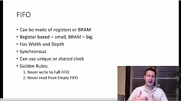
First In First Out is the complete English spelling of FIFO, which means "first in, first out." The term "FIFO" in FPGA or ASIC refers to a memory that stores data in a first-in, first-out manner, and is frequently used for data buffering or high-speed asynchronous data interaction.
The abbreviation FIFO stands for First In First Out in English. It's a first-in, first-out data buffer that's commonly utilized for data buffering or asynchronous data interaction at high speeds. It differs from typical memory in that there is no external read and writes address line, making it very easy to use. However, the downside is that it can only write and read data in sequential order. To finish, the internal read and write pointer automatically adds the data address. The address line, like conventional memory, can be used to read or write to a specific address.
FIFO is a data transfer method that is commonly utilized between various clock zones. For example, one end of the FIFO is used for AD data collecting, while the other is used for the computer's PCI bus. If the AD collection rate is 16-bit 100K SPS, the data volume per second is 100K 16bit=1.6Mbps, and the PCI bus speed is 33MHz, the bus width is 32bit, and the maximum transmission rate is 1056Mbps, the data volume per second is 100K 16bit=1.6Mbps. Between two separate clock zones, FIFO can be utilized as a data buffer. Furthermore, FIFO can be utilized for data interfaces of various widths. Single-chip 8-bit data output, for example, while DSP may be 16-bit data input. FIFO can be utilized to fulfill the goal of data matching when the single-chip and DSP are coupled.
FIFO classification FIFO can be classified as synchronous or asynchronous depending on the clock domain in which it operates. The read clock and the write clock are the same in asynchronous FIFO. When the clock edge comes, read and write operations happen at the same time. The read and write clocks are inconsistent, and the read and write clocks are independent of each other, in asynchronous FIFO.
The challenge with FIFO design is determining when the FIFO is empty or full. It must be assured that the FIFO cannot be written when it is full in order to ensure that the data is accurately written or read without benefit or read-empty status. In the empty state, the read operation is not possible. The question of how to assess whether a FIFO is full or empty has become a central concern in FIFO design.
Ⅱ. How many structures does FIFO have?
Single-clock FIFO (SCFIFO) and dual-clock FIFO (DCFIFO) are the two varieties of FIFO structures, with standard dual-clock (DCFIFO) and mixed-width dual-clock FIFO (DCFIFO MIXED WIDTHS) being the most common. The three FIFO architectures have the following English meanings:
SCFIFO stands for Single Clock FIFO.
• Dual clock FIFO (DCFIFO)
• DCFIFO MIXED WIDTHS: dual clock with mixed width
The mixed-width dual-clock FIFO and dual-clock FIFO are collectively referred to as dual-clock FIFO unless otherwise indicated.
The symbol diagrams of single-clock and dual-clock FIFOs are shown in the figures below:

The single-clock FIFO has a separate clock port clock, as shown in the diagram. The data in data[7..0] is written into the FIFO when the rising edge of Clock comes and wrreq is valid; when the rising edge of Clock arrives and wrreq is valid, the data in data[7..0] is written into the FIFO. If rdreq is genuine, output the data in q[7..0] to the FIFO when it arrives. full is the full flag bit, which is set when the FIFO is full, almost full is the almost full flag, which is set when the FIFO is almost full, and the value of almost full is the value of almost full. It can be configured in the same way as empty and almost empty are empty and almost empty flags, respectively, and almost empty can be configured independently. The data that the current FIFO can use is usedw[7..0]. Sclr is cleared in a synchronized manner. The data in the FIFO is cleared when it is valid and the rising edge of Clocks arrives; aclr is cleared asynchronously, and the data in the FIFO is cleared when it is valid.
Dual-clock FIFOs are similar to single-clock FIFOs in that they employ different clock signals for reading and writing. The full mark is wrfull, and the write empty mark is wrempty. We use wrempty to determine how much data is written in wrusedw[8..0], rdusedw[8..0] when we only want to write when the FIFO is empty .0] What is the maximum amount of data that can be read? When the length of the written data and the length of the read data are different, for example, when the length of the written data is 16 bits and the length of the read data is 8 bits, the written data and the scaled data are tallied separately. The values wrusedw[8..0]=1 and rdusedw[8..0]=2. The full-read flag is rdfull. We can evaluate based on this flag if we only want to read when it is completely full (read data packet). rdempty is a read-only flag that is set when the FIFO contains no viewable data. Please zero aclr asynchronous. Only asynchronous clearing is possible for the dual clock FIFO.
Ⅲ. What are the functions of FIFO of different structures?
FIFO memory is the buffering link of the system. If there is no FIFO memory, the entire system cannot work normally. It has several functions:
1) Cache the continuous data stream to prevent data loss when entering and storing operations;
2) The data is concentrated for stacking and storage, which can avoid frequent bus operations and reduce the burden on the CPU;
3) Allow the system to perform DMA operations to increase the data transmission speed. This is a crucial point. If the DMA operation is not used, the data transmission will not meet the transmission requirements, and the burden on the CPU will be greatly increased, and the data storage work cannot be completed at the same time.
FIFO of different structures has different functions:
Single clock FIFO:
On-chip data exchange frequently employs a single-clock FIFO. For example, under FPGA control, a series of sensor data read from an external sensor is first stored into the FIFO, and then the data is sent out sequentially at the UART serial port's data transmission rate. Because the sensor's single reading data can be very fast, collecting the data is not always essential. For instance, if a sensor uses the SPI interface protocol, the FPGA reads 20 data from the sensor at a 2M SPI data rate, then 9600 data from the sensor. The serial port is used to send the baud rate. Every second, this procedure is carried out. Because the data rate of 2M is substantially higher than the serial port's baud rate of 9600, the data collected from the sensor must first be buffered with FIFO before being sent out slowly at the serial port's data rate. Because the reading of sensor data and the transmission of serial data can both be synchronized with the same clock, this function can be implemented using a single-clock structured FIFO.
Dual clock FIFO:
The transmission and receiving of asynchronous data is a common application of dual-clock FIFO.
The term "asynchronous data" refers to data that is synchronized with distinct clock domains at both the sending and receiving ends. The dual-clock FIFO's separate read and write clock structures can synchronize data from different clock domains to the required clock domain system. The data gathered by the camera, for example, can be shown on the monitor through VGA in a video image acquisition system. The data input by the camera differs in length and speed from the data output to the VGA display. A dual-clock FIFO is employed in this scenario.
Ⅳ. How to use FIFO to implement the functional design in Altera FPGA?
In Altera FPGA, there are three basic techniques to create user function design utilizing FIFO. The first option is for users to create their own FIFO logic based on their requirements. This method can be used to construct FIFO functions when users have specific requirements, but it requires users to have strong RTL design skills. The second option is to employ a third-party IP core that is open source. This IP core is delivered as source code and may be readily integrated into the user's system. When a user has specific needs for the FIFO function, the source code might be used. Make changes to meet your system's requirements. The third option is to take advantage of the Quartus II software's free FIFO IP core. The Quartus II software, in this method, provides users with a user-friendly graphical interface through which they may define numerous FIFO parameters and topologies, as well as the created FIFO IP. The core may also perform structural optimization for various Altera device series.
 UTMEL
UTMEL
We are the professional distributor of electronic components, providing a large variety of products to save you a lot of time, effort, and cost with our efficient self-customized service. careful order preparation fast delivery service
1. What is FIFO?
FIFO is the abbreviation of English First In First Out. It is a first-in-first-out data buffer. The difference between it and ordinary memory is that there is no external read and write address line, so it is very simple to use, but the disadvantage is that it can only write data sequentially. , Sequential read data, the data address is automatically added by the internal read and write pointer to complete, it cannot be read or written to a specified address by the address line as in ordinary memory.
2. How does synchronous FIFO coordinate two different clocks?
Synchronous FIFO has only one clock and does not need to be coordinated. Control read and write with r_en and w_en, read and write one data per clock.
3. What is the size of the FIFO in the FPGA so that memory resources are not wasted?
The bit width of the FIFO setting is consistent with the FPGA you choose, so you can maximize the use of resources.
 Discovering New and Advanced Methodology for Determining the Dynamic Characterization of Wide Bandgap DevicesSaumitra Jagdale15 March 20242703
For a long era, silicon has stood out as the primary material for fabricating electronic devices due to its affordability, moderate efficiency, and performance capabilities. Despite its widespread use, silicon faces several limitations that render it unsuitable for applications involving high power and elevated temperatures. As technological advancements continue and the industry demands enhanced efficiency from devices, these limitations become increasingly vivid. In the quest for electronic devices that are more potent, efficient, and compact, wide bandgap materials are emerging as a dominant player. Their superiority over silicon in crucial aspects such as efficiency, higher junction temperatures, power density, thinner drift regions, and faster switching speeds positions them as the preferred materials for the future of power electronics.
Read More A Comprehensive Guide to FPGA Development BoardsUTMEL11 September 202521020
This comprehensive guide will take you on a journey through the fascinating world of FPGA development boards. We’ll explore what they are, how they differ from microcontrollers, and most importantly, how to choose the perfect board for your needs. Whether you’re a seasoned engineer or a curious hobbyist, prepare to unlock new possibilities in hardware design and accelerate your projects. We’ll cover everything from budget-friendly options to specialized boards for image processing, delve into popular learning paths, and even provide insights into essential software like Vivado. By the end of this article, you’ll have a clear roadmap to navigate the FPGA landscape and make informed decisions for your next groundbreaking endeavor.
Read More 800G Optical Transceivers: The Guide for AI Data CentersUTMEL24 December 202511534
The complete guide to 800G Optical Transceiver standards (QSFP-DD vs. OSFP). Overcome supply shortages and scale your AI data center with Utmel Electronic.
Read More The 2026 Engineer’s Guide: Choosing the Right MCU for Your Next IoT & New Energy ProjectUTMEL30 April 20261131
A comprehensive comparison of 2026's leading MCUs from ST, NXP, and Microchip across power efficiency, processing performance, connectivity, and ecosystems to help engineers select the optimal chip for next-gen IoT and new energy projects.
Read More AI Server Components: Engineering Next-Gen Data Center Hardware for 100kW RacksUTMEL15 May 2026524
The transition from traditional enterprise IT to AI-driven workloads has rendered legacy data center hardware obsolete, forcing infrastructure planners to re-engineer server components for extreme thermal environments.
Read More
Subscribe to Utmel !
![MOC3020VM]() MOC3020VM
MOC3020VMON Semiconductor
![HCS201T/SN]() HCS201T/SN
HCS201T/SNMicrochip Technology
![DLP6500BFYE]() DLP6500BFYE
DLP6500BFYETexas Instruments
![80HCPS1432CHMGI]() 80HCPS1432CHMGI
80HCPS1432CHMGIRenesas Electronics America Inc.
![MOC3082SVM]() MOC3082SVM
MOC3082SVMON Semiconductor
![DLP9500BFLN]() DLP9500BFLN
DLP9500BFLNTexas Instruments
![LTC3725EMSE#TRPBF]() LTC3725EMSE#TRPBF
LTC3725EMSE#TRPBFLinear Technology/Analog Devices
![MC68882RC50A]() MC68882RC50A
MC68882RC50ANXP USA Inc.
![LTC4213IDDB#TRMPBF]() LTC4213IDDB#TRMPBF
LTC4213IDDB#TRMPBFLinear Technology/Analog Devices
![FM31276-GTR]() FM31276-GTR
FM31276-GTRCypress Semiconductor Corp


